8-bit Computer in FPGA
Computers are mysterious. These machines have always been so enigmatic to most people. I can guarantee that if you ask someone on the road how computers work, they would most likely just answer “I don’t know”.
I was like that for a long time, even after I started learning programming. So I decided that I will learn how a computer works by building one.
At first, I was thinking about building a breadboard computer like Ben Eater. But then I realized that I don’t really have access to a lot of the components that Ben used where I live so I decided to make this computer using software, and since I just started learning Verilog, I decided to put my Verilog skill to the test by making this computer.
The toolchain
For this project, I decided to use some open source toolchain for FPGA. When I was doing some research, I found Apio, which is an open source ecosystem of FPGA tools, so I decided to use Apio for this project.
Here’s how you install Apio:
- Install Python
- Install Apio with
pip(if thepipcommand is not available, runeasy_install pip)
$ pip install -U apio
- Install necessary packages:
$ apio install -a
Now you can use Apio for your project. Check out Apio’s quick start page to learn how to use it.
The architecture
I based this computer’s architecture on the SAP-1 in Digital Computer Electronics.
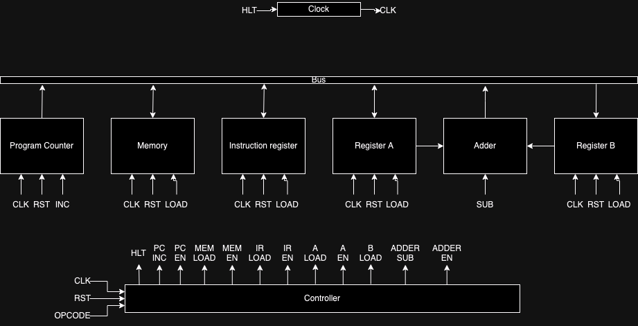
The modules share some common signal path: clk, rst and out.
- clk: The clock signal
- rst: The reset signal (resets everything back to 0)
- out: The output of each modules (connected to the bus for communication between modules)
I combined the MAR module from the original SAP-1 architecture with the RAM module to make the memory module. Some signals may also have different names as I’m basing the architecture of this computer off of my memory of the SAP-1 architecture.
This won’t be an exact copy of the SAP-1 but it’s close enough and it’s still a functioning 8-bit computer.
So let’s get to making this computer.
The components
Let’s see how each components of the computer works:
- The bus: This is where all the data is sent through. It is 8-bit wide and it is how components communicate with and send data to each other. The bus have enable signals that will allow it to multiplex between the different outputs of the modules.
- The clock: This module synchronizes all the components. Think of it like a conductor leading an orchestra. This component will output the clk_in signal if hlt is low, and output 0 if hlt is high. The hlt signal is used to implement the HLT instruction later on.
- The program counter: This module holds the next instruction to be executed. This module counts from
0x0to0xFas there’s only 16 bytes of memory in this computer. The inc signal tells this module to increment the value in itself by 1. - The instruction register: This module loads the instruction from memory and seperates the opcode and the data. The upper 4 bits of the instruction is the opcode and the lower 4 bits is the address of the data. For the instructions that don’t require data (like HLT), the lower 4 bits will be ignored.
- The accumulator (A register): This is the main register of the computer. This stores the intermediate data during an execution. This needs a load signal to load values into it from the bus.
- The B register: This a buffer register used to perform arithmetic operations. It’s basically a supporting register for the A register. It holds the number to be added to or subtracted from the A register. It also accepts a load signal to load values into it from the bus.
- The adder: This module is responsible for doing all the math in this computer. It can add (A + B) or subtract (A - B). It doesn’t use the clock signal as it is constantly calculating and outputing the result based on the A and B values.
- The memory: There’s 16 bytes of memory in this computer. The memory has a 4-bit register called the Memory Address Register or MAR for short, which temporarily holds a memory address of data or instruction in memory. This stored address is sent to the RAM where data and instructions are read from. It takes the computer 2 cycles to read from memory: 1st cycle will load an address from the bus into the MAR, 2nd cycle will use the value in the MAR to address into the RAM and output the value. This computer will initialize the memory by loading from a file called program.bin
- The controller: This is the most complicated part about the computer. It will decide what the computer will do next by asserting different control signals in a 12-bit control word at different execution stages. We’ll talk about the different control signals and execution stages later on.
The execution stages
Instruction execution occurs in a series of stages (each stage takes 1 clock cycle). This computer has 6 stages (0 to 5). It counts up to 5 then goes back to 0 then continue (counts using a 3-bit register)
Opcode is passed from the instruction register into the controller to do things based on what instruction is. Output of the controller is the 12 control signals used to control all the other modules. Different stages of different instructions will assert different signals to accomplish different things.
Control signals:
- hlt: halt execution
- pc_inc: increment program counter
- pc_en: put value of the pc onto the bus
- mar_load: load address into memory address register
- mem_en: put value from memory into the bus
- ir_load: load value from bus into intruction register
- ir_en: put value in ir onto the bus
- a_load: load value from bus into A register
- a_en: put value in A onto the bus
- b_load: load value from bus into B register
- adder_sub: subtract value in B from A
- adder_en: put value in adder onto the bus
The instructions
This computer has 4 instructions:
| Opcode | Instruction | Description |
|---|---|---|
| 0000 | LDA $x | Load value at memory location $x into A |
| 0001 | ADD $x | Add value at memory location $x with value in A and store the sum in A |
| 0010 | SUB $x | Subtract value at memory location $x from value in A and store the difference in A |
| 1111 | HLT | Halt program execution |
Every instruction has the same first 3 stages:
- Stage 0: Put the PC onto bus and load that value into MAR (pc_en -> mar_load)
- Stage 1: Increment PC (pc_inc)
- Stage 2: Put value in memory at the MAR address onto the bus and load that into the IR (mem_en -> ir_load)
Next 3 stages differs from instruction to instruction:
| Stage | LDA | ADD | SUB | HLT |
|---|---|---|---|---|
| Stage 3 | Put instruction operand onto the bus and load that value into MAR (ir_en -> mar_load) | Put instruction operand onto the bus and load that value into MAR (ir_en -> mar_load) | Put instruction operand onto the bus and load that value into MAR (ir_en -> mar_load) | Halt the clock (hlt) |
| Stage 4 | Put value in memory at the MAR address onto the bus and load that into the A register (mem_en -> a_load) | Put value in memory at the MAR address onto the bus and load that into the B register (mem_en -> b_load) | Put value in memory at the MAR address onto the bus and load that into the B register (mem_en -> b_load) | Idle |
| Stage 5 | Idle | Put value in the adder onto the bus and load that into the A register (adder_en -> a_load) | Subtract then put the value in the adder onto the bus and load that into the A register (adder_sub -> adder_en -> a_load) | Idle |
The Verilog modules
These modules will be programmed in Verilog. There will be a top module that will be used to connect all of these components together. There will also be a top module testbench to test out the design and check if the computer is working or not.
The clock
module clock(
	input hlt, // halt signal
	input clk_in,

	output clk_out
);

	assign clk_out = hlt ? 1'b0 : clk_in;

endmodule
The program counter
module pc(
	input clk,
	input rst,
	input inc,

	output[7:0] out
);

	reg[3:0] pc;

	always @ (posedge clk, posedge rst)
	begin
		if (rst)
		begin
			pc <= 4'b0;
		end else if (inc)
		begin
			pc <= pc + 1;
		end
	end

	assign out = pc;

endmodule
The instruction register
module ir(
	input clk,
	input rst,
	input load,
	input[7:0] bus,

	output[7:0] out
);

	reg[7:0] ir;

	always @ (posedge clk, posedge rst)
	begin
		if (rst)
		begin
			ir <= 8'b0;
		end else if (load)
		begin
			ir <= bus;
		end
	end

	assign out = ir;

endmodule
The accumulator (A register)
module reg_a(
	input clk,
	input rst,
	input load,
	input[7:0] bus,

	output[7:0] out
);

	reg[7:0] reg_a;

	always @ (posedge clk, posedge rst)
	begin
		if (rst)
		begin
			reg_a <= 8'b0;
		end else if (load)
		begin
			reg_a <= bus;
		end
	end

	assign out = reg_a;

endmodule
The B register
module reg_b(
	input clk,
	input rst,
	input load,
	input[7:0] bus,

	output[7:0] out
);

	reg[7:0] reg_b;

	always @ (posedge clk, posedge rst)
	begin
		if (rst)
		begin
			reg_b <= 8'b0;
		end else if (load)
		begin
			reg_b <= bus;
		end
	end

	assign out = reg_b;

endmodule
The adder
module adder(
	input[7:0] a,
	input[7:0] b,
	input sub,

	output[7:0] out
);

	assign out = sub ? a - b : a + b;

endmodule
The memory
module memory(
	input clk,
	input rst,
	input load,
	input[7:0] bus,

	output[7:0] out
);

	// setting memory
	initial begin
		$readmemh("program.bin", ram);
	end

	reg[3:0] mar;
	reg[7:0] ram[0:15];		// 16 8-bit wide elements

	always @ (posedge clk, posedge rst)
	begin
		if (rst)
		begin
			mar <= 4'b0;
		end else if (load)
		begin
			mar <= bus[3:0];
		end
	end

	assign out = ram[mar];

endmodule
The controller
/*
Control signals:
	hlt: halt execution
	pc_inc: increment program counter
	pc_en: put value of the pc onto the bus
	mar_load: load address into memory address register
	mem_en: put value from memory into the bus
	ir_load: load value from bus into intruction register
	ir_en: put value in ir onto the bus
	a_load: load value from bus into A register
	a_en: put value in A onto the bus
	b_load: load value from bus into B register
	adder_sub: subtract value in B from A
	adder_en: put value in adder onto the bus
*/

module controller(
	input clk,
	input rst,
	input[3:0] opcode,

	output[11:0] out
);

	localparam HLT = 11;
	localparam PC_INC = 10;
	localparam PC_EN = 9;
	localparam MAR_LOAD = 8;
	localparam MEM_EN = 7;
	localparam IR_LOAD = 6;
	localparam IR_EN = 5;
	localparam A_LOAD = 4;
	localparam A_EN = 3;
	localparam B_LOAD = 2;
	localparam ADDER_SUB = 1;
	localparam ADDER_EN = 0;

	localparam OP_LDA = 4'b0000;
	localparam OP_ADD = 4'b0001;
	localparam OP_SUB = 4'b0010;
	localparam OP_HLT = 4'b1111;

	reg[2:0] stage;
	reg[11:0] ctrl_word;

	always @ (posedge clk, posedge rst)
	begin
		if (rst)
		begin
			stage <= 0;
		end else
		begin
			if (stage == 5)
			begin
				stage <= 0;
			end else
			begin
				stage <= stage + 1;
			end
		end
	end

	always @ (*)
	begin
		ctrl_word = 12'b0;

		case (stage)
			0:
				begin
					ctrl_word[PC_EN] = 1;
					ctrl_word[MAR_LOAD] = 1;
				end
			1:
				begin
					ctrl_word[PC_INC] = 1;
				end

			2:
				begin
					ctrl_word[MEM_EN] = 1;
					ctrl_word[IR_LOAD] = 1;
				end

			3:
				begin
					case (opcode)
						OP_LDA:
                            begin
                                ctrl_word[IR_EN] = 1;
                                ctrl_word[MAR_LOAD] = 1;
                            end

                        OP_ADD:
                            begin
                                ctrl_word[IR_EN] = 1;
                                ctrl_word[MAR_LOAD] = 1;
                            end

                        OP_SUB:
                            begin
                                ctrl_word[IR_EN] = 1;
                                ctrl_word[MAR_LOAD] = 1;
                            end

                        OP_HLT:
                            begin
                                ctrl_word[HLT] = 1;
                            end
                    endcase
				end
            4:
                begin
                    case (opcode)
                        OP_LDA:
                            begin
                                ctrl_word[MEM_EN] = 1;
                                ctrl_word[A_LOAD] = 1;
                            end

                        OP_ADD:
                            begin
                                ctrl_word[MEM_EN] = 1;
                                ctrl_word[B_LOAD] = 1;
                            end

                        OP_SUB:
                            begin
                                ctrl_word[MEM_EN] = 1;
                                ctrl_word[B_LOAD] = 1;
                            end
                    endcase
                end

            5:
                begin
                    case (opcode)
                        OP_ADD:
                            begin
                                ctrl_word[ADDER_EN] = 1;
                                ctrl_word[A_LOAD] = 1;
                            end

                        OP_SUB:
                            begin
                                ctrl_word[ADDER_SUB] = 1;
                                ctrl_word[ADDER_EN] = 1;
                                ctrl_word[A_LOAD] = 1;
                            end
                    endcase
                end
        endcase
	end

    assign out = ctrl_word;

endmodule
The top module
module top_design(
	input CLK
);

	reg[7:0] bus;

	// multiplex between the output of the different modules
	always @ (*)
	begin
		if (ir_en)
		begin
			bus = ir_out;
		end else if (adder_en)
		begin
			bus = adder_out;
		end else if (a_en)
		begin
			bus = a_out;
		end else if (mem_en)
		begin
			bus = mem_out;
		end else if (pc_en)
		begin
			bus = pc_out;
		end else
		begin
			bus = 8'b0;
		end
	end

    // generate clock signal
    wire rst;
    wire hlt;
    wire clk;
    clock clock (
        .hlt(hlt),
        .clk_in(CLK),
        .clk_out(clk)
    );


    // program counter
    wire pc_inc;
    wire pc_en;
    wire[7:0] pc_out;
    pc pc(
        .clk(clk),
        .rst(rst),
        .inc(pc_inc),
        .out(pc_out)
    );


    // memory
    wire mar_load;
    wire mem_en;
    wire[7:0] mem_out;
    memory mem(
        .clk(clk),
        .rst(rst),
        .load(mar_load),
        .bus(bus),
        .out(mem_out)
    );


    // A register (accumulator)
    wire a_load;
    wire a_en;
    wire[7:0] a_out;
    reg_a reg_a(
        .clk(clk),
        .rst(rst),
        .load(a_load),
        .bus(bus),
        .out(a_out)
    );


    // B register
    wire b_load;
    wire[7:0] b_out;
    reg_b reg_b(
        .clk(clk),
        .rst(rst),
        .load(b_load),
        .bus(bus),
        .out(b_out)
    );


    // adder
    wire adder_sub;
    wire adder_en;
    wire[7:0] adder_out;
    adder adder(
        .a(a_out),
        .b(b_out),
        .sub(adder_sub),
        .out(adder_out)
    );


    // instruction register
    wire ir_load;
    wire ir_en;
    wire[7:0] ir_out;
    ir ir(
        .clk(clk),
        .rst(rst),
        .load(ir_load),
        .bus(bus),
        .out(ir_out)
    );


    // controller
    controller controller(
        .clk(clk),
        .rst(rst),
        .opcode(ir_out[7:4]), // upper 4 bits
        .out(
        {
            hlt,
            pc_inc,
            pc_en,
            mar_load,
            mem_en,
            ir_load,
            ir_en,
            a_load,
            a_en,
            b_load,
            adder_sub,
            adder_en
        })
    );

endmodule
The top module testbench
module top_design_tb();

    initial begin
        $dumpfile("top_design_tb.vcd");
        $dumpvars(0, top_design_tb);

        // pulse reset signal
        rst = 1;
        #1
        rst = 0;
    end

    // multiplexer
    wire[4:0] bus_en = {pc_en, mem_en, ir_en, a_en, adder_en};
    reg[7:0] bus;
    always @ (*)
    begin
        case (bus_en)
            5'b00001: bus = adder_out;
            5'b00010: bus = a_out;
            5'b00100: bus = ir_out;
            5'b01000: bus = mem_out;
            5'b10000: bus = pc_out;
            default: bus = 8'b0;
        endcase
    end

    // clock signal
    reg clk_in = 0;
    integer i;
    initial begin
        for (i = 0; i < 128; i++)
        begin
            #1
            clk_in = ~clk_in;
        end
    end

    wire clk;
    wire hlt;
    reg rst;
    clock clock(
        .hlt(hlt),
        .clk_in(clk_in),
        .clk_out(clk)
    );

    wire pc_inc;
    wire pc_en;
    wire[7:0] pc_out;
    pc pc(
        .clk(clk),
        .rst(rst),
        .inc(pc_inc),
        .out(pc_out)
    );

    wire mar_load;
    wire mem_en;
    wire[7:0] mem_out;
    memory mem(
        .clk(clk),
        .rst(rst),
        .load(mar_load),
        .bus(bus),
        .out(mem_out)
    );


    wire a_load;
    wire a_en;
    wire[7:0] a_out;
    reg_a reg_a(
        .clk(clk),
        .rst(rst),
        .load(a_load),
        .bus(bus),
        .out(a_out)
    );


    wire b_load;
    wire[7:0] b_out;
    reg_b reg_b(
        .clk(clk),
        .rst(rst),
        .load(b_load),
        .bus(bus),
        .out(b_out)
    );


    wire adder_sub;
    wire adder_en;
    wire[7:0] adder_out;
    adder adder(
        .a(a_out),
        .b(b_out),
        .sub(adder_sub),
        .out(adder_out)
    );


    wire ir_load;
    wire ir_en;
    wire[7:0] ir_out;
    ir ir(
        .clk(clk),
        .rst(rst),
        .load(ir_load),
        .bus(bus),
        .out(ir_out)
    );

    controller controller(
        .clk(clk),
        .rst(rst),
        .opcode(ir_out[7:4]),
        .out(
        {
            hlt,
            pc_inc,
            pc_en,
            mar_load,
            mem_en,
            ir_load,
            ir_en,
            a_load,
            a_en,
            b_load,
            adder_sub,
            adder_en
        })
    );

endmodule
The program
Finally, to program the computer, we can program the bytes directly into a file named program.bin. This file will get loaded into the memory module when the computer starts. Here’s an example program:
0D 2E 1F F0 00 00 00 00 00 00 00 00 00 05 04 02
This is the annotated version of the example program:
$0      0D      // LDA $D   Load A with the value at address $D
$1      1E      // ADD $E   Add the value at address $E to A
$2      2F      // SUB $F   Subtract the value at address $F from A
$3      F0      // HLT      Stop execution
$4      00      // Padding byte
$5      00      // Padding byte
$6      00      // Padding byte
$7      00      // Padding byte
$8      00      // Padding byte
$9      00      // Padding byte
$A      00      // Padding byte
$B      00      // Padding byte
$C      00      // Padding byte
$D      05      // Data
$E      04      // Data
$F      02      // Data
And after all of that, we have the end result, a functioning 8-bit computer:
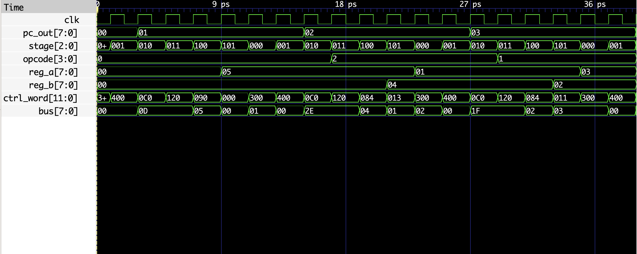
We can see that the data in reg_a is getting added and subtracted with the data in reg_b just like how we programmed it in program.bin.
You can find the source code here.